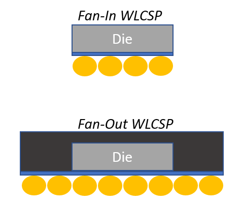
FlipChip top, Wafer level chip packaging technology PCB HERO top, WLCSP 9 P2 Packages Nisshinbo Micro Devices top, Wafer Level Packaging Services For 3D IC Flip Chip WLCSP top, What is Wafer Level Packaging WLP Wafer Level Chip Scale top, Wafer Level Chip Size Package WLCSP Guidelines EEWeb top, Design Manufacturing and Handling Guidelines for Cypress Wafer top, Amkor Technology Inc. Amkor s WLCSP package family is top, WLCSP Jiangsu CAS Microelectronics Integration Technology Co Ltd top, WLCSP MOSFETs WLCSP MOSFETs Nexperia top, InPlay Unveils World s Smallest Bluetooth SoC in WLCSP Package top, Chip scale package Wikipedia top, Wafer Level Chip Size Package WLCSP Guidelines EEWeb top, News Winbond leads the era of wearable devices with the launch top, Image Sensors World Development of Reliable WLCSP for Automotive top, WAFER LEVEL CHIP SCALE PACKAGE WLCSP top, WLCSP Overview Market and Applications AnySilicon top, Are WLCSP the Solution during Silicon Shortage MCU on Eclipse top, Semiconductor Back end Process 3 Packages top, Exploring WLCSP Package Wafer Level Chip Scale Packaging IBE top, Hand soldering a WLCSP package top, WLCSP Overview Market and Applications AnySilicon top, FlipChip top, Schematic drawing of a wafer level chip scale package WLCSP top, Figure 1 from Board Level Reliability Enhancement of WLCSP with top, Faraday Technology Corporation WLCSP Testing Bumping Process top, AN3846 Wafer Level Chip Scale Package WLCSP Application Note top, WLCSP Wafer Level CSP Wafer Level Packaging Amkor Technology top, WLCSP Zero to ASIC Course top, Eng Sub Wafer Level Chip Scale Package WLCSP top, WL CSP or WLCSP Wafer level Chip Scale Packaging MADPCB top, Structure of compliant bump WLCSP Download Scientific Diagram top, WLCSP Zero to ASIC Course top, The schematic of the package a 3D view of the CIS WLCSP top, Bluetooth Low Energy Design QFN or WLCSP Argenox top, Product Info: Wlcsp top
.
Wlcsp top